PCB DESIGN & LAYOUT.
Professional PCB design and layout services for reliable and high-performance electronic products.
ENGINEERING CORE.
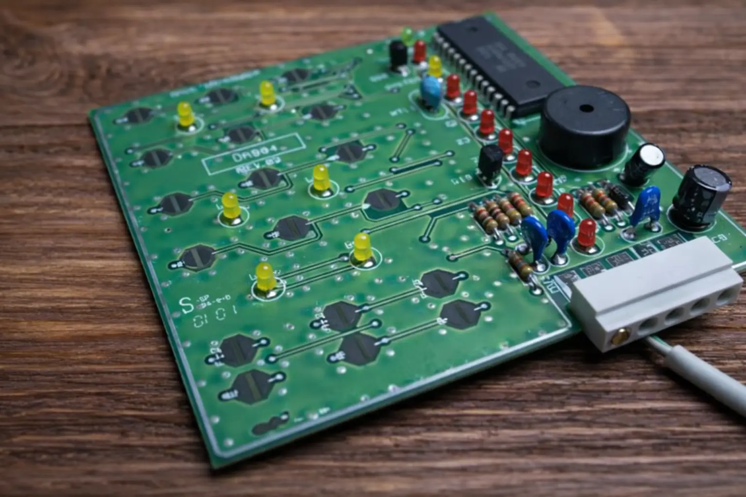
At Mech Volt Innovations, we understand that PCB design and layout are critical to the performance, reliability, and manufacturability of any electronic product. Our PCB design engineers bring deep expertise in schematic capture, component placement, signal integrity analysis, and layout optimisation for both simple and complex multi-layer boards. We design PCBs that meet your electrical performance requirements, adhere to manufacturing design rules, and are optimised for the specific operational environment of your product.
Core Capabilities
KEY BENEFITS
Compact Form Factors
High-density multi-layer routing to fit complex electronics into small enclosures.
Signal Integrity
Optimised layouts that prevent cross-talk and maintain clean data transmission.
Manufacturability (DFM)
Boards designed strictly according to fab-house limitations to prevent unbuildable designs.
Our Process
Schematic Capture
Translating system requirements into a logical, error-free electronic schematic.
Component Placement
Strategically placing components to minimize trace lengths and thermal hotspots.
Routing & Planes
Executing multi-layer routing while maintaining strict impedance and clearance rules.
Gerber Generation
Exporting standardized manufacturing files (Gerbers, Drill files, Pick & Place).